





- A +
- A
- A -
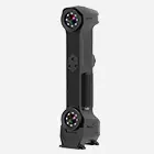
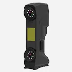
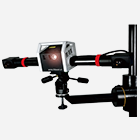
Reverse modeling is required for the circuit boards of a certain factory. In the past, reverse modeling for PCB circuit boards mostly adopted manual caliper measurement, camera‑based board copying, physical delamination and disassembly and other methods, which were low‑efficiency. A high‑precision industrial 3D scanner is used to perform full‑area data acquisition of the outer contour of the PCB and the layout of electronic components. Point cloud processing and reverse‑modeling software are applied to reconstruct the 3D model, providing accurate digital references for circuit replication and structural design.

现场图
1. Poor accuracy and significant errors. Industrial PCBs feature micro‑components, fine traces and tiny vias. Manual mapping cannot capture micron‑level precision data, resulting in large dimensional deviations and easily distorted coordinate points.
2. Low efficiency and high destructiveness. Traditional reverse‑engineering of PCBs requires grinding for layer separation and layer‑by‑layer mapping, which takes from several days to weeks and is extremely inefficient. In addition, physical disassembly tends to damage inner‑layer copper foils and traces, rendering samples scrapped and making it impossible to preserve the complete structure of the original board.
3. Limited data and weak reusability. Traditional PCB cloning only outputs two‑dimensional planar data. It fails to restore three‑dimensional parameters such as board thickness, three‑dimensional layout of components and pad height. It merely enables simple duplication and cannot support secondary‑development work including simulation analysis, structural optimization, modification and iteration.

Point cloud data STL diagram
To address the above‑mentioned pain points, a non‑contact industrial 3D scanning reverse‑engineering solution is adopted in this work to realize non‑destructive, high‑precision and rapid reverse modeling of PCBs. With no physical contact or PCB disassembly required, the scanner can clearly capture all 3D features of the circuit board, including its outer contour, mounting hole positions, positions and heights of electronic components, and the shapes of connectors. Complete high‑density point cloud data can be acquired within 10 minutes with an accuracy of 0.02 mm. Geometric features such as planes, circular holes and rectangular boundaries are automatically identified and fitted in the software, so that critical parameters including mounting hole diameters, hole‑position coordinates, overall board dimensions, and component heights can be obtained accurately. Based on the extracted feature data and point‑cloud mesh, a solid 3D model of the PCB is reconstructed in reverse‑engineering modeling software, which fully restores the outer boundaries, matrix of mounting holes, component layout and height‑restricted areas. The model can be exported to universal formats such as STP, IGS and CAD, and directly applied for structural interference checking, thermal simulation, jig design or housing adaptation development.

Reverse‑modeling STP drawing
Solution Effectiveness: Compared with traditional processes, this solution realizes non‑destructive reverse engineering of PCBs, improves modeling accuracy by more than 90%, and shortens the operation cycle by 80%. It effectively addresses the challenges of accurate reproduction and iteration of PCB boards, and provides reliable digital support for the maintenance of industrial equipment, spare‑parts production and product upgrading.